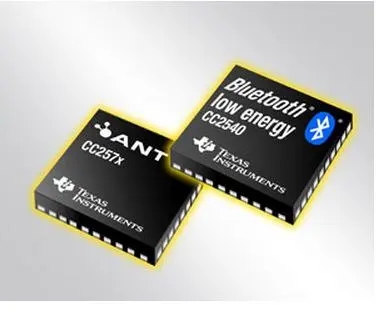
CC2540
FEATURES
True Single-Chip BLE Solution: CC2540 Can Run Both Application and BLE Protocol
Stack, Includes Peripherals to Interface With Wide Range of Sensors, Etc.6-mm × 6-mm Package
RF
Bluetooth low energy technology Compatible
Excellent Link Budget (up to 97 dB), Enabling Long-Range
Applications Without External Front EndAccurate Digital Received Signal-Strength Indicator (RSSI)
Suitable for Systems Targeting Compliance With Worldwide
Radio Frequency Regulations: ETSI EN 300 328 and
EN 300 440 Class 2 (Europe), FCC CFR47
Part 15 (US), and ARIB STD-T66 (Japan)Layout
Few External Components
Reference Design Provided
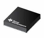
6-mm × 6-mm QFN40 Package
Low Power
Active Mode RX Down to 19.6 mA
Active Mode TX (–6 dBm): 24 mA
Power Mode 1 (3-µs Wake-Up): 235 µA
Power Mode 2 (Sleep Timer On): 0.9 µA
Power Mode 3 (External Interrupts): 0.4 µA
Wide Supply Voltage Range (2 V–3.6 V)
Full RAM and Register Retention in All Power Modes
TPS62730 Compatible
Low Power in Active ModeRX Down to 15.8 mA (3 V Supply)
TX (-6 dBm): 18.6 mA (3 V Supply)
Microcontroller
High-Performance and Low-Power 8051 Microcontroller Core
In-System-Programmable Flash, 128 KB or 256 KB
8-KB SRAM
Peripherals
12-Bit ADC with Eight Channels and Configurable Resolution
Integrated High-Performance Op-Amp and Ultralow-Power Comparator
General-Purpose Timers (One 16-Bit, Two 8-Bit)
21 General-Purpose I/O Pins (19× 4 mA, 2× 20 mA)
32-kHz Sleep Timer With Capture
Two Powerful USARTs With Support for Several Serial Protocols
Full-Speed USB Interface
IR Generation Circuitry
Powerful Five-Channel DMA
AES Security Coprocessor
Battery Monitor and Temperature Sensor
Each CC2540 Contains a Unique 48-bit IEEE Address
Software Features
CC2540 Mini Development Kit
SmartRF Software
Supported by IAR Embedded Workbench Software for 8051
Complete Power-Optimized Stack, Including Controller and
HostSample Applications and Profiles
Multiple Configuration options
BTool – Windows PC Application for Evaluation, Development, and Test
GAP – Central, Peripheral, Observer, or Broadcaster
(Including Combination Roles)ATT / GATT – Client and Server
SMP – AES-128 Encryption and Decryption
L2CAP
Generic Applications for GAP Central and Peripheral Roles
Proximity, Accelerometer, Simple Keys, and Battery GATT Services
Single-Chip Configuration, Allowing Application to Run on CC2540
Network Processor Interface for Applications Running on an External Microcontroller
Bluetooth v4.0 Compliant Protocol Stack
for Single-Mode BLE SolutionDevelopment Tools
APPLICATIONS
2.4-GHz Bluetooth low energy Systems
Mobile Phone Accessories
Sports and Leisure Equipment
Consumer Electronics
Human Interface Devices (Keyboard, Mouse, Remote Control)
USB Dongles
Health Care and Medical
CC2540 with TPS62730
TPS62730 is a 2 MHz Step Down Converter with Bypass Mode
Extends Battery Lifetime by up to 20%
Reduced Current in TX and RX
30 nA Bypass Mode Current to Support Low Power Modes
RF Performance Unchanged
Small Package Allows for Small Solution Size
CC2540 Controllable